Semiconductor Metrology & Inspection Equipment Market: The Role of Government Initiatives
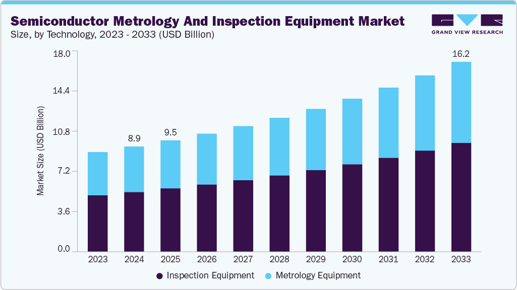
The global semiconductor metrology and inspection equipment market was valued at USD 8.98 billion in 2024 and is expected to grow to USD 16.21 billion by 2033.
The global semiconductor metrology and inspection equipment market was valued at USD 8.98 billion in 2024 and is expected to grow to USD 16.21 billion by 2033, reflecting a CAGR of 6.9% from 2025 to 2033. This growth is largely driven by the increasing complexity of semiconductor devices, such as FinFETs, Gate-All-Around (GAA) transistors, and 3D NAND architectures, which demand advanced metrology and inspection tools to ensure optimal yield and performance.
Additionally, the rising adoption of EUV (Extreme Ultraviolet) lithography, increased investments in sub-7nm process technologies, and the expansion of global semiconductor fabrication (fab) capacity, particularly in Asia-Pacific and North America, are contributing to the growing need for high-precision in-line and 3D metrology systems.
A significant factor fueling this growth is the U.S. government's investment in semiconductor technology through the CHIPS & Science Act. Since 2022, the Act has allocated over USD 100 million toward advanced metrology research and an additional USD 300 million for next-generation packaging metrology, in collaboration with the National Institute of Standards and Technology (NIST) and Manufacturing USA. These initiatives are supporting the development of inspection tools capable of handling sub-5 nm geometries, promoting domestic manufacturing and strengthening R&D in semiconductor technologies. This funding is accelerating innovation and commercializing cutting-edge metrology solutions.
Another important factor driving growth in the semiconductor metrology market is the increasing emphasis on standardized, traceable measurements. Leading organizations like Germany’s PTB, the UK’s NPL, and the U.S. NIST are working to create robust calibration systems for semiconductor applications across a range of wavelengths, from EUV to infrared. PTB’s Metrology Light Source (MLS) facility, for example, plays a crucial role in enabling high-accuracy calibration for semiconductor tools. These traceability efforts are enhancing consistency across global fab environments and improving interoperability, which in turn is boosting the adoption of metrology and inspection systems worldwide.
Order a free sample PDF of the Semiconductor Metrology And Inspection Equipment Market Intelligence Study, published by Grand View Research.
Key Market Trends & Insights
- Asia Pacific led the semiconductor metrology and inspection equipment market with a 54.7% revenue share in 2024. This dominance is driven by rapid fab expansions and increased investment in advanced process nodes across Taiwan, South Korea, China, and Japan. Government-backed technology roadmaps and industrial policies have turned the Asia Pacific region into a hub for semiconductor equipment procurement, especially for tools focused on 3D inspection, high-throughput metrology, and EUV mask analysis.
- Inspection Equipment was the largest market segment, accounting for 56.8% of revenue in 2024. The need for early defect detection in advanced manufacturing nodes is propelling this demand. Optical and electron beam inspection systems are critical for identifying defects during lithography and etching, which are key for maintaining high yield and throughput, especially as devices shrink.
- 2D Metrology/Inspection tools dominated the market in 2024 but are expected to see slower growth as the industry shifts toward more complex 3D architectures. These tools are still crucial for legacy and mid-range process nodes (28 nm and above) but will face increasing competition from 3D-based solutions as chip designs become more vertically integrated.
- The ≤ 7 nm process node segment was the largest revenue driver in 2024. This segment is growing due to the increasing demand for precision in applications like high-performance computing (HPC), artificial intelligence (AI), and mobile systems on chips (SoCs). As the industry moves toward 5 nm, 3 nm, and eventually 2 nm nodes, the need for advanced inspection and metrology tools to handle line-edge roughness, pattern collapse, and EUV mask defects will continue to grow.
- Foundries accounted for the largest market revenue share by fab type in 2024, driven by the diverse customer applications and the continuous migration of technology to advanced nodes. Leading foundries are adopting new metrology and inspection tools to support a wide range of technologies, from mature process nodes to cutting-edge geometries.
Market Size & Forecast
- 2024 Market Size: USD 8.98 Billion
- 2033 Projected Market Size: USD 16.21 Billion
- CAGR (2025-2033): 6.9%
- Asia Pacific: Largest market in 2024
Key Companies & Market Share Insights
Notable players in the semiconductor metrology and inspection equipment market include KLA Corporation, Applied Materials, Inc., Hitachi High-Tech Corporation, and ASML. These companies are investing heavily in developing advanced tools for sub-7 nm and 3D packaging nodes. As semiconductor device architectures become more complex, with new challenges such as gate-all-around FETs and chiplet integration, these companies are pushing the boundaries of precision measurement, offering atomic-scale resolution and real-time defect classification.
- KLA Corporation is a global leader in semiconductor metrology, with a diverse portfolio that includes optical and electron beam inspection, critical dimension scanning electron microscopy (CD-SEM), overlay metrology, and defect review systems. KLA is also at the forefront of AI-driven analytics and real-time defect classification for sub-5 nm and 3D chip architectures.
- Applied Materials, Inc. is another key player offering integrated metrology and inspection solutions. The company’s innovations in inline measurement systems using advanced optics, quantum sensors, and AI algorithms help monitor and control critical parameters during chip fabrication. Applied is also focusing on next-generation technologies, such as gate-all-around transistors and 3D packaging, to enhance yield and process accuracy.
Key Players
- Applied Materials, Inc.
- ASML
- Camtek
- Hitachi High-Tech Corporation
- KLA Corporation
- Lasertec Corporation
- Nova Ltd.
- Onto Innovation
- SCREEN Semiconductor Solutions Co., Ltd.
- Thermo Fisher Scientific Inc.
Explore Horizon Databook – The world's most expansive market intelligence platform developed by Grand View Research.
Conclusion
The semiconductor metrology and inspection equipment market is on a strong growth trajectory, driven by the increasing complexity of chip architectures and advancements in process technologies. As the industry progresses toward smaller process nodes and more intricate device structures, the demand for high-precision metrology and inspection tools will continue to grow. Key market drivers include government investments, such as the U.S. CHIPS & Science Act, and the push for standardized, traceable measurements to ensure consistency across global semiconductor fabs. Leading companies in the sector are adapting to these trends by developing next-generation solutions that support the shift to sub-7 nm nodes, 3D packaging, and advanced defect detection.