Advanced PCB Materials and Techniques for Next-Gen Telecommunication Devices
Explore advanced PCB materials and assembly techniques for next-gen telecommunication devices. Learn how precise pcb manufacturing and assembly boosts performance.
The rapid evolution of telecommunication devices demands cutting-edge PCB manufacturing and assembly practices. As devices become faster, smaller, and more complex, manufacturers must adopt advanced materials and techniques to meet performance and reliability requirements. This article explores the latest trends in PCB materials and assembly processes that are shaping next-generation telecommunication solutions.
Why Advanced PCB Materials Matter
In telecommunication devices, the PCB is the backbone of performance. The choice of material affects:
- Signal integrity: High-frequency signals require low dielectric constant (Dk) and low dissipation factor (Df) materials to prevent signal loss.
- Thermal management: Devices operating at high speeds generate significant heat, necessitating materials with excellent thermal conductivity.
- Mechanical durability: PCBs must withstand vibration, shock, and repeated thermal cycles without degradation.
Common advanced materials include:
FR-4 High-Speed Laminates: Standard for many telecommunication PCBs but upgraded for higher frequency applications.
Rogers Laminates: Ideal for RF and microwave devices due to low Dk and Df values.
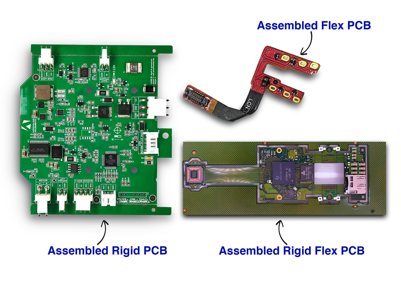
Polyimide Films: Used in flexible and rigid-flex PCBs for their heat resistance and mechanical flexibility.
Metal Core PCBs: Provide superior thermal dissipation, essential for high-power components.
Key Techniques in PCB Manufacturing and Assembly
Modern pcb manufacturing and assembly goes beyond traditional fabrication. Several advanced techniques enhance performance and reliability:
1. High-Density Interconnect (HDI) Design
HDI PCBs include microvias, blind vias, and buried vias to increase wiring density without enlarging the board size. Benefits include:
- Smaller, lightweight devices
- Improved signal performance
- Reduced power consumption
2. Multilayer PCB Construction
Next-gen telecommunication devices often require multilayer boards, sometimes exceeding 12 layers, to accommodate complex circuits. Advantages include:
- Compact designs with high functionality
- Reduced electromagnetic interference (EMI)
- Easier integration of RF components
3. Advanced Soldering Techniques
Reliable soldering is critical in pcb board assembly manufacturing. Techniques include:
- Surface Mount Technology (SMT): Allows components to be placed directly on the PCB surface for higher density and precision.
- Through-Hole Technology (THT): Provides stronger mechanical connections for heavy or high-stress components.
- Reflow and Wave Soldering: Ensures consistent solder joints for both SMT and THT components.
4. Thermal Management Solutions
High-speed telecommunication devices generate heat that must be managed effectively. Advanced techniques include:
- Thermal vias: Channels heat away from critical components.
- Metal-core boards: Dissipate heat more efficiently than traditional FR-4 boards.
- Heat sinks and copper pours: Reduce hotspots on densely populated boards.
Emerging Trends in PCB Materials
The telecommunication industry is continuously innovating, resulting in new materials that improve performance, durability, and reliability:
- Low-Loss Laminates: Reduce signal degradation in RF and high-speed applications.
- Flexible and Rigid-Flex PCBs: Enable compact device designs and dynamic assembly possibilities.
- Environmentally Friendly Materials: Lead-free, halogen-free laminates that meet global compliance standards.
- Nano-Enhanced Materials: Improve electrical and thermal properties for demanding telecommunication applications.
Quality Assurance in PCB Board Assembly Manufacturing
Ensuring high-quality assembly is as important as advanced materials. Key quality practices include:
- Automated Optical Inspection (AOI): Detects soldering defects and component misalignment.
- X-ray Inspection: Checks hidden solder joints, especially in BGA and microvia designs.
- Functional Testing: Simulates operational conditions to ensure reliability.
- Cleanroom Assembly: Reduces contamination that can cause failures in high-frequency applications.
Benefits of Advanced PCB Techniques for Telecommunication Devices
Adopting advanced PCB manufacturing and assembly methods offers several benefits for next-generation telecommunication devices:
- Enhanced Signal Integrity: Low-loss materials and precise assembly reduce interference and data errors.
- Miniaturisation: HDI and multilayer PCBs allow smaller device footprints without sacrificing functionality.
- Higher Reliability: Thermal management and quality assurance reduce failure rates in demanding environments.
- Faster Time-to-Market: Efficient assembly techniques streamline production cycles.
Best Practices for Telecommunication PCB Manufacturing
Manufacturers should follow best practices to achieve optimal results:
- Use high-quality, validated materials for high-frequency applications.
- Employ HDI and multilayer designs to meet space and performance constraints.
- Integrate thermal management strategies early in the design phase.
- Ensure robust testing and inspection throughout assembly to guarantee reliability.
- Partner with experienced PCB board assembly manufacturing providers for precision and consistency.
Conclusion
The demands of next-generation telecommunication devices require advanced PCB materials and techniques. From low-loss laminates and HDI designs to precise assembly and rigorous quality control, these strategies ensure high performance, reliability, and efficiency. Adopting these practices in pcb manufacturing and assembly allows manufacturers to create devices capable of supporting faster networks, smaller form factors, and more complex functionalities.
By focusing on material innovation, cutting-edge assembly techniques, and stringent quality assurance, the future of telecommunication devices is not just faster—it’s smarter and more reliable.